1.Introduction to Semiconductor Talent Training at NKUST
The semiconductor-related courses offered by National Kaohsiung University of Science and Technology are designed around industry needs and practical applications, with the goal of cultivating technology professionals equipped with semiconductor expertise, hands-on skills, innovative research capabilities, and a global perspective. The curriculum balances advanced research with practical implementation and integrates laboratory training and industry–academia collaboration to develop students’ abilities in integrated circuit design and engineering problem-solving. It also emphasizes interdisciplinary collaboration, teamwork, communication, and the study of international literature. By combining university resources with industry expertise, the curriculum aims to bridge the gap between academic learning and professional practice, prepare students for careers in the semiconductor industry, and contribute to technological innovation and industrial advancement.
2.Professional Courses
2.1 For Undergraduate Students
2.2 For Graduate Student
3.Equipment and Instrument
Located at the Nanzih Campus of National Kaohsiung University of Science and Technology (NKUST), the Semiconductor Process Equipment Talent Development Center comprises five specialized laboratories: the Semiconductor General Skills Lab, the Semiconductor Instrumentation and Control Integration Lab, the Semiconductor Process Equipment Lab, the Semiconductor Vacuum System Lab, and the Semiconductor Metrology Lab.
As the semiconductor industry continues to expand, securing skilled production-line technicians has become a top human resources priority for major companies. Recognizing this critical need, NKUST, with the support of Taiwan's Ministry of Education, established this state-of-the-art training facility in 2025.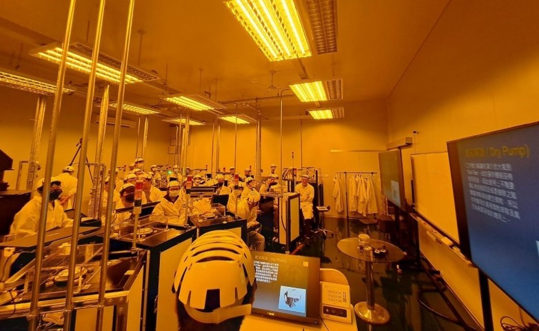
Figure Caption: Students are trained on vacuum system instrumentation modules and wafer handling robotics. To replicate real-world semiconductor industry standards, students are required to wear safety helmets, hold maintenance tools, and don cleanroom garments. This Semiconductor Instrumentation and Control Integration Lab fully simulate an authentic amber lighting environment.
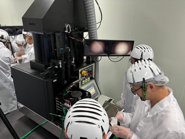
Figure Caption: The semiconductor lithography process from mask design to wafer printing. Through a practical, hands-on educational approach, students progress from foundational exposure theory to the actual maintenance and troubleshooting of lithography exposure tools
At the Jiangong Campus of National Kaohsiung University of Science and Technology (NKUST), Professor Ting-Jen Hsueh of the Department of Electronic Engineering leads students in operating an automatic die bonder and a sputtering deposition system. The training covers die positioning, pick-and-place bonding, thin-film deposition, process parameter configuration, and equipment fault diagnosis. Drawing on Professor Hsueh’s expertise in semiconductor devices, MEMS sensors, and nano-device technologies, the program combines on-site demonstrations with hands-on equipment training to develop the operational and troubleshooting skills required in semiconductor production environments.
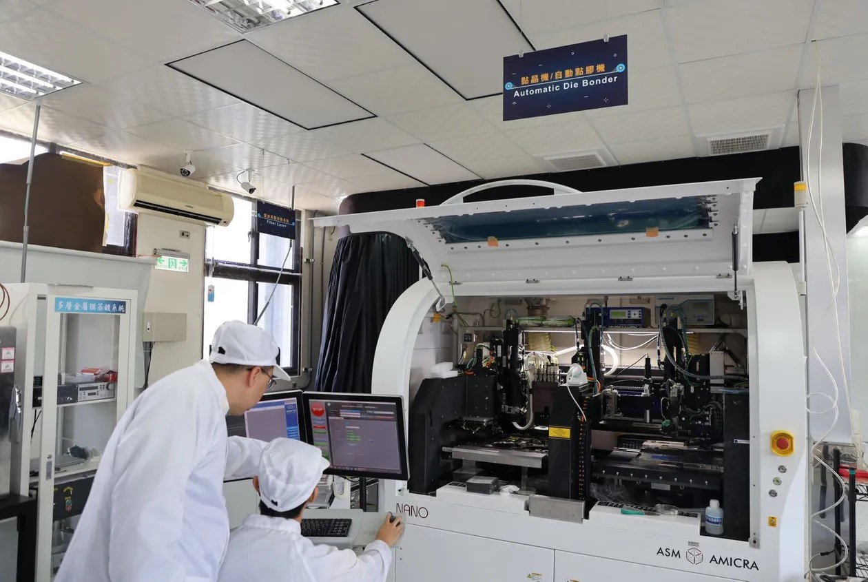
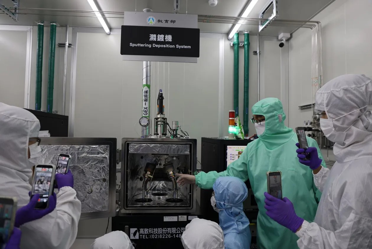
Figure Caption: Professor Yu-Hung Chen of the Department of Microelectronics Engineering (pictured in the green cleanroom suit) explains the internal component configuration of a vacuum sputtering chamber, demonstrating to students how the thin-film deposition process occurs following plasma source generation and target bombardment.
4.Visitors
In March 2026, an industrial delegation from Mie Prefecture, Japan, visited the Department of Semiconductor Engineering at National Kaohsiung University of Science and Technology (NKUST) to learn about the university’s semiconductor facilities, practice-oriented curriculum, and talent development achievements. NKUST also introduced its training center, which is capable of preparing approximately 300 technically skilled professionals each year. The visit focused on semiconductor talent exchange and industry–academia collaboration, highlighting the university’s capacity to connect with international industries and cultivate highly qualified semiconductor professionals.
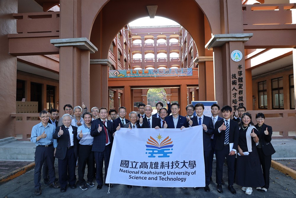
Industrial partners from Japan visit the Semiconductor Process Equipment Talent Development Base at NKUST
Located in Room 6108 of the Daren Building at NKUST’s Nanzih Campus, the Semiconductor Vacuum Systems Laboratory is supported by senior equipment engineers and managers from Tianhong Technology, Gaodun Technology, and United Microelectronics Corporation (UMC). Students receive hands-on training in vacuum pumps, vacuum gauges, and RF power calibration instruments, while learning evacuation procedures, pressure monitoring, system calibration, and equipment troubleshooting. The laboratory provides practical experience closely aligned with semiconductor production environments and strengthens students’ capabilities in equipment operation, maintenance, and fault diagnosis.
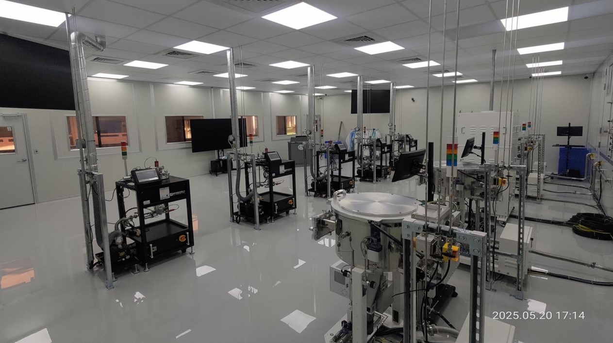
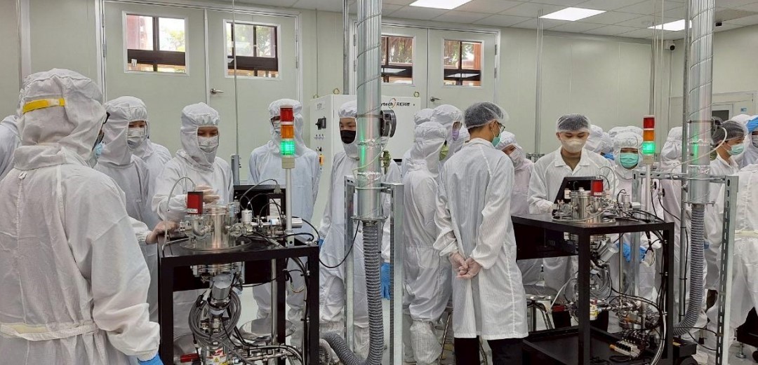
Figure Caption: The upper image features a commercial-grade 12-inch wafer plasma processing system currently used in the industry, while the lower image shows a low-pressure or vacuum processing system. Both systems represent indispensable technologies for manufacturing advanced nanoscale chips, and both machines are proudly made in Taiwan. Our fully-equipped laboratory allows students to work in small groups, ensuring every student gets hands-on experience learning the mechanical architecture of the equipment.
Through its industry–academia partnership with United Microelectronics Corporation (UMC), National Kaohsiung University of Science and Technology (NKUST) provides students with opportunities to gain first-hand exposure to semiconductor enterprises. During company visits, students learn about wafer fabrication processes, equipment engineering roles, facility management, and real-world production environments, allowing them to connect classroom knowledge with industrial practice. Since 2023, NKUST and UMC have jointly promoted semiconductor equipment talent development, with UMC engineers participating in practical instruction and offering company visits, internship opportunities, and career pathways. These initiatives help students identify their professional goals at an early stage and reduce the learning gap when entering the semiconductor industry.
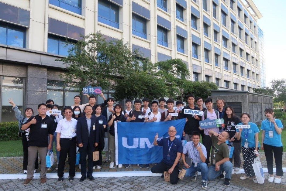
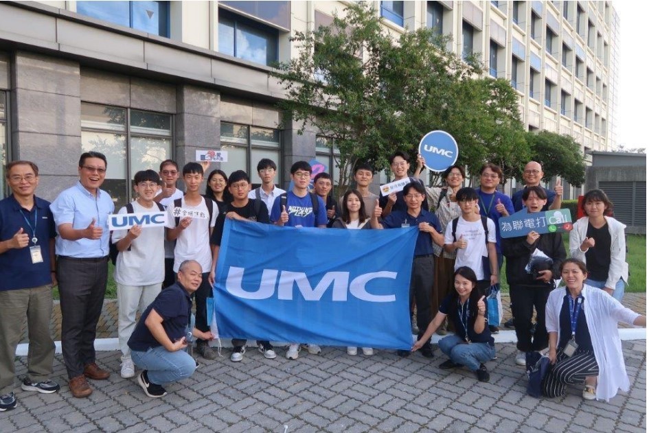
Student visit UMC Semiconductor Company
The Ministry of Education, in collaboration with National Kaohsiung University of Science and Technology (NKUST) and ASE Technology Holding, established an industry-oriented training facility for semiconductor packaging and testing. Through donated equipment and a production-line simulation environment, the facility brings packaging, testing, equipment maintenance, and process management directly into the university curriculum. Students can reinforce theoretical knowledge while gaining hands-on experience in equipment operation, quality inspection, and troubleshooting under conditions closely aligned with industrial practice. Industry professionals also contribute to curriculum development, practical instruction, company visits, and internship programs, ensuring that training responds directly to workforce needs. This collaboration integrates educational resources, NKUST’s academic expertise, and Kaohsiung’s semiconductor industry cluster, helping to bridge the gap between education and employment while strengthening NKUST’s role in developing semiconductor professionals for southern Taiwan.
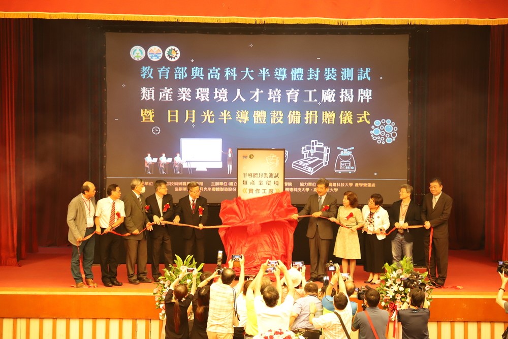
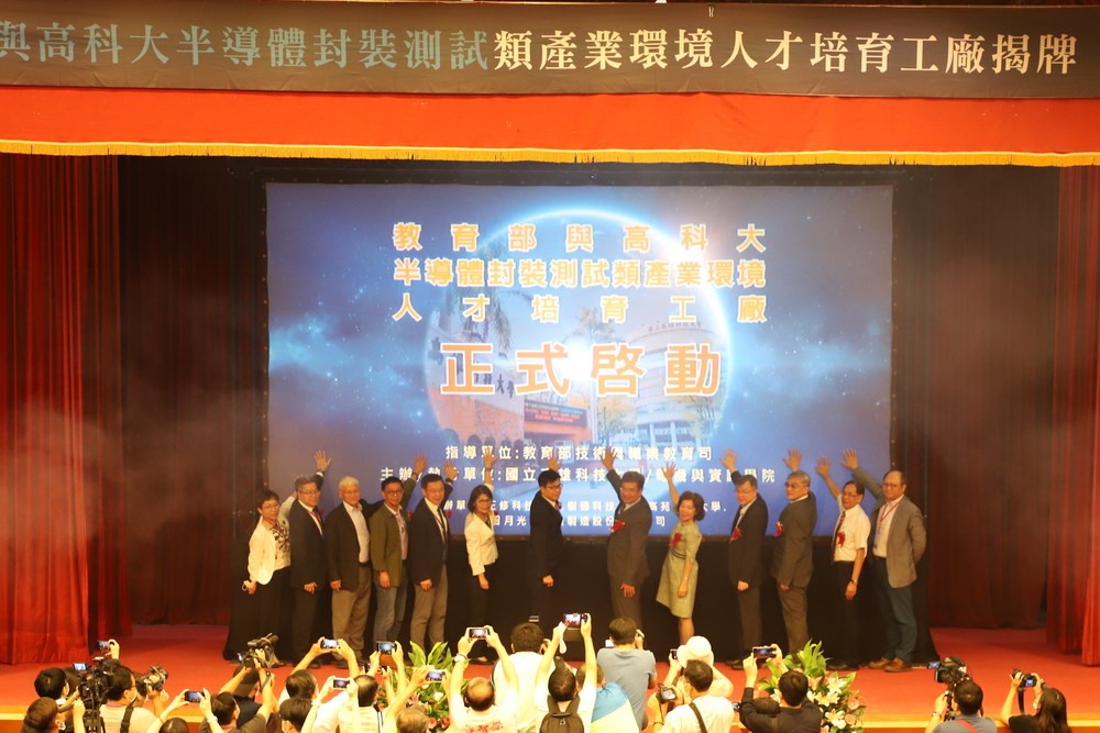
Opening ceremony of Semiconductor Training Center supported by Ministry of Education, Taiwan.
5.Research and Development
[1] M.-F. Tsai, S.-H. Fan, and T.-J. Hsueh, “Manufacture of a stable MEMS gas sensor using radio-frequency sputtering deposition and the hyperthermal annealing of GaOₓ/CuInGaSe₂ films,” Sens. Actuators B Chem., vol. 442, Art. no. 138130, Nov. 2025, doi: 10.1016/j.snb.2025.138130.
[2] Y.-R. Chen, S.-J. Chang, and T.-J. Hsueh, “A co-planarized common cathode micro-LED display that is produced using planarization and a copper process,” IEEE Electron Device Lett., vol. 45, no. 10, pp. 1875–1878, Oct. 2024, doi: 10.1109/LED.2024.3442436.
[3] M.-F. Tsai, R.-Y. Ding, and T.-J. Hsueh, “Optimized gallium oxide/MEMS gas sensor for H₂S gas detection that exhibits increased sensitivity and stability,” Appl. Surf. Sci., vol. 696, Art. no. 162944, 2025, doi: 10.1016/j.apsusc.2025.162944.
[4] M.-F. Tsai et al., “Comparative study of the sensitivity of H₂S and NO₂ in CuInSe₂ gas sensors that are fabricated using screen printing and MEMS integration,” Appl. Surf. Sci., vol. 676, Art. no. 160995, 2024, doi: 10.1016/j.apsusc.2024.160995.
[5] C.-W. Huang, C.-Y. Wu, and T.-J. Hsueh, “A room temperature ZnO:Ga NWs&NSs/MEMS H₂S gas sensor,” Mater. Sci. Semicond. Process., vol. 187, Art. no. 109149, Mar. 2025, doi: 10.1016/j.mssp.2024.109149.
[6] Z.-H. Shi, Y.-J. Hsiao, S.-P. Chang, and S.-J. Chang, “Synthesis and characterization of an oxygen-controlled CuO/SnO₂ sensor for NO₂ detection,” Sens. Actuators B Chem., vol. 421, Art. no. 136517, Dec. 2024, doi: 10.1016/j.snb.2024.136517.
[7] T.-Y. Wang, W.-C. Lai, Q.-J. Xie, S.-P. Chang, C.-H. Kuo, and J.-K. Sheu, “Thermally oxidized AlₓGa₂₋ₓO₃/n-Al₀.₆Ga₀.₄N:Si unipolar resistive random-access memory,” ACS Appl. Electron. Mater., vol. 6, no. 5, pp. 3688–3694, 2024, doi: 10.1021/acsaelm.4c00365.
[8] W.-C. Hung, J.-F. Chang, S.-P. Chang, S.-J. Chang, and J.-C. Chen, “Using hybrid bonding for stacked bi-color micro-light-emitting diodes,” IEEE Trans. Compon. Packag. Manuf. Technol., vol. 15, no. 9, pp. 1886–1889, 2025, doi: 10.1109/TCPMT.2025.3595581.
[9] H.-Y. Liu et al., “Fabrication of high efficiency green InGaN/GaN microLEDs by modulating potential barrier height of the sidewall MQWs in V-pits,” IEEE Photon. J., vol. 16, no. 3, Art. no. 8200409, Jun. 2024, doi: 10.1109/JPHOT.2024.3386111.
[10] J.-F. Chang, W.-C. Hung, S.-P. Chang, J.-C. Chen, and S.-J. Chang, “Efficiency and precision performance of laser bonding technology in micro-LED packaging processes,” IEEE Trans. Compon. Packag. Manuf. Technol., vol. 16, no. 5, pp. 1166–1169, May 2026, doi: 10.1109/TCPMT.2026.3675699.
[11] C.-H. Chen, T.-Y. Yang, Y.-Y. Chen, and S.-B. Liu, “Influence of DNA solution on dark and deep-UV response of Ga₂O₃/p-Si Schottky diodes,” IEEE Photon. Technol. Lett., early access, 2026, doi: 10.1109/LPT.2026.3693070.
[12] Y.-Y. Chen, C.-H. Chen, S.-B. Liu, and C.-C. Chien, “Influence of ultrathin NiSi embedded in AZO films on electrical and optical properties,” Vacuum, vol. 252, Art. no. 115437, 2026, doi: 10.1016/j.vacuum.2026.115437.
[13] C.-H. Chen, S.-B. Liu, and T.-C. Wang, “Photosensitive characteristics of Ga₂O₃/p-Si Schottky barrier solar-blind photodetector,” IEEE Photon. J., vol. 17, no. 5, Art. no. 6801507, Oct. 2025, doi: 10.1109/JPHOT.2025.3607986.
[14] C.-H. Chen, S.-B. Liu, and S.-P. Chang, “Performance improvement of a ZnGa₂O₄ extended-gate field-effect transistor pH sensor,” ACS Omega, vol. 9, no. 13, pp. 15304–15310, Mar. 2024, doi: 10.1021/acsomega.3c09965.
[15] S.-B. Liu, C.-H. Chen, S.-Y. Cheng, and C.-Y. Kuo, “Low cost sputtered gallium oxide pH sensor based on open circuit potential measurement,” in Proc. 2025 IEEE Int. Conf. Consumer Electronics–Taiwan (ICCE-Taiwan), 2025, doi: 10.1109/ICCE-Taiwan66881.2025.11207983.
[16] W. Hidayat, P.-H. Tseng, J.-H. Liu, and J.-J. Jou, “Design and verification of a 53-Gb/s PAM-4 cooled DFB-LD TOSA employing cost-effective TO-CAN package,” IEEE Access, vol. 13, pp. 155855–155864, 2025, doi: 10.1109/ACCESS.2025.3605604.
[17] W. Hidayat, P.-H. Chen, C.-L. Yang, J.-Y. Yeh, C.-P. Chao, and J.-J. Jou, “Design and fabrication of a four-channel CWDM cooled DFB-LD module with OSFP electrical interface for CPO external laser sources,” Opt. Continuum, vol. 4, no. 8, pp. 1719–1731, Aug. 2025, doi: 10.1364/OPTCON.569826.
[18] J.-J. Jou, P.-Y. Wang, B.-H. Liu, C.-L. Yang, and C.-L. Tseng, “Wide-range tunable ring VCO with band-switching in 0.18-µm CMOS technology,” Circuits Syst. Signal Process., vol. 45, no. 5, pp. 3369–3383, 2026, doi: 10.1007/s00034-025-03384-3.
[19] J.-J. Jou, C.-L. Yang, C.-L. Tseng, C.-C. Yao, and J.-Y. Zheng, “Real-time monitoring of high-speed signal quality using asynchronous sampling, amplitude sorting, and artificial neural network and its FPGA implementation,” Int. J. Circuit Theory Appl., vol. 53, no. 12, pp. 7260–7270, 2025, doi: 10.1002/cta.4557.
[20] P.-Y. Wang, J.-H. Liu, B.-Z. Zhang, T.-L. Hsieh, and J.-J. Jou, “Four-channel 200 Gb/s PAM-4 electro-absorption-modulated laser module,” IET Conf. Proc., vol. 2025, no. 15, pp. 174–176, 2025, doi: 10.1049/icp.2025.2523.
[21] C.-Y. Liu, C.-Y. Yang, H.-G. Chiu, D.-H. Du, and Z.-L. Lee, “Analog resistive switching and synaptic behavior of Ni/TiOₓ/TiOᵧ/TiN structures for artificial intelligence computing,” presented at the 17th Int. Symp. Sputtering and Plasma Processes (ISSP 2024), Kyoto, Japan, Jul. 2–5, 2024, Paper P3-04.
[22] C.-L. Lee, “Investigation of resistive switching and synaptic characteristics in bilayer HfOₓ structures,” M.S. thesis, Dept. Electron. Eng., National Kaohsiung Univ. Sci. Technol., Kaohsiung, Taiwan, 2025.
[23] D.-H. Du, “Resistive switching and electronic synaptic characteristics of ZnO-based RRAM,” M.S. thesis, Dept. Electron. Eng., National Kaohsiung Univ. Sci. Technol., Kaohsiung, Taiwan, 2025.
[24] H.-G. Chiu, “Resistive switching and electronic synapse characteristics of Al/HfOₓ/ZnOᵧ/TiN stacked structure,” M.S. thesis, Dept. Electron. Eng., National Kaohsiung Univ. Sci. Technol., Kaohsiung, Taiwan, 2024.
[25] C.-H. Huang, “Growth of MoS₂ by sulfidation method and investigation of chemical doping on its piezoresistive characteristics,” M.S. thesis, Dept. Electron. Eng., National Kaohsiung Univ. Sci. Technol., Kaohsiung, Taiwan, 2023.
Contact: College of Electrical, Electronic and Computer Science
Email: waoffice01@nkust.edu.tw